Wednesday, 16 August 2017

Flashing Intel Edison Firmware Manually

Hello everyone
Generally, we flash Intel Edison Boards with Intel Edison Board Configuration Tool on Windows 10/Windows 7. But, sometimes,while we are flashing the Yocto Linux Image on Edison board, it fails!!. At that time, we must do a manual flash of image.

Open Windows command prompt for manual installation.Go to folder where image is available, unpack the image, download “dfu-util-0.9” or latest version for windows from given link, download dfu-util-0.9-win64.zipextract file “dfu-util” and “libusb-1.0.dll” and paste in the same folder of image.
Now, using command prompt, go the directory where the extracted image was stored, run “flashall.bat” on command prompt. It should come like this:


·         Once It is done, do not immediately remove cable. Leave it for 2-4 min. Disconnect the board and again open the Intel Edison Board Configuration Tool. This time, the Firmware option in tool must be green which signifies that board is successfully installed with latest firmware.


·         If by any case, Firmware/Image does not get installed (still yellow color) in this method, Firmware might have got corrupted and re-flash need to be done. In such case, we should take few extra steps:

      1. Connect board to laptop, access board using Teraterm/Putty/MobaXTerm using COM USB.
      2. Set Serial Baud rate to 115200 and boot board with existing firmware.
      3. When you come across following message, press key to enter in boot mode


      Stop the autoboot process on the Edison and get the the "boot >" prompt. Once you're at the "boot >" prompt, type "run do_flash". You should see the following output:
      Saving Environment to MMC...
      Writing to redundant MMC(0)... done
      GADGET DRIVER: usb_dnl_dfu
      Once you see the "GADGET DRIVER: usb_dnl_dfu" message, the Edison board is in the correct state to accept flashing again. 

       Now use, windows command prompt to reach to the directory where extracted Yocto image is placed  and files “dfu-util” and “libusb-1.0.dll” are copied and pasted as explained in beginning of post. Run  from the following command "flashall.bat". This would re-flash your firmware from beginning and make  your board re-usable. 

      This is tried and tested method and gives 100% result... Try for yourself !
       Happy Learning :-)

Monday, 7 August 2017

Role of APIs, System calls & Device Drivers explained with example

Here, we are going to talk about API, System calls and device drivers. Lets start with API first.

API (Application Programming Interface): API are the functions or entry points provided by any application or system to use its features. Application developer need not to reinvent the wheel, he just uses the API available and manage to use the feature of different applications in his own application.ex. using Google map API in your application to identify location for given latitude and longitude.
From system perspective, application developer uses the system API to access certain features or resources provided by system in simplified manner. Application developer need not to develop the process or method to access the system so his job is simplified and fast. ex. accessing ram space by any application

System calls: System calls are the entry point to kernel space so that any application can talk to kernel and make it understand what is needed by them.ex. we can use google apis to access location in any application but sohow this intend is to told to kernel so that it can further talk to processor about same and make hardware work for application requirements. Actual work have to done by hardware anyhow, so it must be requested from it to activate GPS and find the exact latitude and longitude. Another example could be copying set of contents into file. Actual work of copying dat have to carried out by processor and system calls help to inform kernel that 'now' copy action need to be performed from where to where....

Device Driver: This piece of code would help processor talk to specific hardware in 'right' manner so that exactly what is intended is what is done by hardware. Take the same example of google apis. Here, processor need to talk to GPS and ask it to fetch the exact latitude and longitude rather than fetching area name. So Device Driver helps to establish talk between processor and hardware and let it perform the right task.

Now, linking all three in same example.....Google apis (API) would be used by application named 'GPS tracker' to fetch and latitude and longitude, which would inform kernel about this activity via system calls. Further kernel would inform processor about same and then processor uses correct device driver in right manner to get the location with help of GPS hardware. Now this latitude and longitude given by GPS hardware would be passed from processor to kernel, from kernel to API via system call and finally displayed on the 'Google Tracker' application.

Hope I have made myself clear :-)

Lets keep learning! Please post your comments below :-)

Working principle of Triple-axis Accelerometer

Slide 1
Welcome to webinar series on Intel Higher Education Challenge 2017. In this webinar, we are going to learn about I2C protocol and it implementation for Gesture recognition using ADXL345 three axis accelerometer
Slide 2
In this webinar, we are going to learn about following topics:
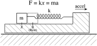
Lets understand the physics of acceleration measurement in Accelerometer using spring and mass systems. Springs generally obey Hooke's law. If this system undergoes an acceleration, then by using Newton's 2nd law and force conserving equation, we get F = ma = kx


F=kx, where k is the constant of proportionality (spring coefficient) between displacement (x) and force (F).
Hence an acceleration a will cause the mass to be displaced by
                                          x=ma/k    -------------- (i) 
alternatively, if we observe a displacement of x, we know that the mass has undergone an acceleration of
                                         a=kx/m      --------------- (ii)

Thus, if we can somehow measure displacement x, we can measure the actual acceleration a on the body.
For accelerometers that use the MEMS technology, two approaches for measuring dominate the market: (i) capacitive sensing, (ii) piezoelectric sensing.

These approaches convert mechanical information into electrical signals by methods that are particular to the silicon technology.
The case of measuring using the capacitive mechanism is considered next
                                                                                                                                                                                                 
A change in causes a change in the capacitance defined by                            
                                   C=ε_0  A/xa                ---------- (iii)
where ε_0 is the permittivity of the air gap, and A is the surface area on either side of the proof mass where the springs are located, xa is the distance between capacitor plate and mass m.
By varying the distance xa , we can vary capacitance ‘C’. Combining Equation  (ii) & (iii), we can find acceleration  ‘a’ in mass ‘m’.
               a=(k.A.ε_0)/mC         --------------- (iv)
This way, you can calculate acceleration in all three axis x, y and z coordinates.
Hope this explination helped many of you to understand the basic physics behind working of accelerometers.

Happy Learning! Please post your comments below :-)


Wednesday, 21 September 2016

Understading Process, Tasks and Threads in Operating Systems

In my experience, I have seen many beginners baffling around the role of Process and Task. Whether they are same or different ? Is different how, and if same, why it is needed to give two different name for similar entity?
In this article, I have tried to give simple explanation about these basic concepts of Operating Systems which would hopefully make you understand the importance of each entity at basic level.

Process: 

  • Always used in context to General Purpose Operating Systems (GPOS) ex: Linux or Windows. 
  • It an instance of program or application currently in execution
  • Process are generally large in number in any GPOS.
  • Whenever process is created, all necessary resources required for smooth execution of process is allocated by OS.
  • Every process believes that it can access dedicated address space of 4GB (2^32=4GB), for 32-bit processor but due to unavailability of sufficient physical address space, virtual memory concept is introduced and Memory Management Unit (MMU) comes into picture for virtual memory to physical memory translation.
  • There is a fair chance that process may modify/affect the address space assigned to other  to process so MMU must be involved which segregate the process address space by allocating different virtual address spaces to every process.
  • Due to this Virtual memory to physical memory translation, no process can know the actual physical address range of other chances (due to different offset values), process address range overlap chances becomes minimal and each of the processes can work smoothly.  
  • Ex: google chrome is an application, and flash plugin or any plugin we use in chrome can be considered as an independent process; even if one process crashes, other process is not affected!

Task:

  • This word is used mostly while discussing on Real Time Operating Systems
  • Task is considered similar to process in terms of its behaviour but certainly at the level lower to process but no where equivalent to thread.
  • Analogy could be given to a man , who stays as father in his home, but in office works as employee and in his friend circle, a helpful friend and sincere neighbour. Now in this example, even though the man is same but his role changes as per situation and place. Similar thing happens with process/task. In GPOS, it plays the role of process (demanding) and in RTOS, it plays a role of task (relatively less demanding).
  • A task is also an instance of application which is currently in execution just like a while loop in an application. 
  • Task is similar to process in terms of its conceptualisation but it differs in the way it behaves in RTOS
  • In RTOS, due to less number of parallel applications runing, number of task are significantly less than any GPOS, which makes the task management relatively easier for programmer so it does not need any virtual memory requirement.
  • Since virtual memory is not needed, no virtual to physical translation in needed which removes any need of MMU.
  • Removing the requirement of MMU lowers the system cost and also reduces the extra burden of translation, thus improves the response time of system and helping it be Real Time.

This discussion would be left without talking on threads, so lets have a very brief overview on thread 
Thread:
  • This entity is again used in GPOS 
  • This is considered as light weight process since it does not demand for independent data memory and heap memory as every process does. Thread do have its own stack memory.
  • Instead, it shares these memories which helps them for better inter thread communication
  • Thread cannot exist independently
  • There can be multiple threads in any process.

Live example:
Consider MS Office as one big application, which contains Ms-Word, Ms-Powerpoint, MS-Excel etc. as independent programs. These programs may be considered as independent process, which is created as if needed by user. Now when we write on MS-word, say, there are many things happening in background ex: auto-save, indentation, spell check, punctuation, etc. each of this work is governed by individual threads.

Hope this article would have given you some basic clarification of Process, Tasks and Threads.

Happy learning :-)

Sunday, 10 April 2016

Delay calculation using 8085 microprocessor

Hello friends
Lets understand the process of delay calculation in 8085 using following example. We need to calculate the exact duration in microseconds or milliseconds which would be provided by given delay routine.

Let's assume that 8085 is running at 2MHz frequency so
1 clock duration (T) = 1/f = 0.5usec

1                 MVI B, 10H     7 T-States
2 LOOP2    MVI C, FFH     7 T-States
3 LOOP1    DCR C              4 T-States
4                 JNZ LOOP1    10 T-States
5                 DCR B              4 T-States
6                 JNZ LOOP2    10 T-States

Now start calculation

NOTE: Always remember to start from inner most loop and then move towards outer loop.

In this program, for sake of simplicity, I have also associated line numbers

Steps:

1) 1st innermost loop is at line no. 3 and 4. Now line 3 and 4 is going to get repeated for FFH or 256 times i.e. (10+4) T-states would be repeated for256 times. But since, in the last itteration, JNZ condition fails and JZ instruction gets executed. JNZ instruction takes 10 T-states whereas JZ takes 7 T-states. So for 14 T-states are processed for 254 iterations, but in 255th iteration, it took only 11 T-states, so while calculation:
  
        (255 x 14) - 3 = 3567 T-states

2) Now, these 3567 T-states, along with (7+4+10) T-states are placed in another outer loop, which is going to rotate for 10H times or 16 times. Don't forget to subtract 3 for the same reason mentioned in point 1.

        ( (3567 + 7 + 4 + 10) x 16) - 3 = 57405 T-states

3) Now, combine this value to the T-state of 1st instruction of delay routine

         (57405+7) = 57412 T-state

4) Since 1 clock duration = 1 T-state = 0.5usec, so

          (57412 x 0.5usec) = 28.706 msec

This given routine is going to generate delay of 28.706 msec. This same process is applied to calculate the execution time of any 8085 microprocessor program such that user can calculate how responsive system might be, if the system is running using given program and said specification.

Happy learning :-) Please post your comments below!

8085 Timing Diagram detailed explaination using example.

Hi friends
What exactly timing diagram tell us?? It tells us the internal behavior of microprocessor while instruction gets processed. Microprocessor generates certain signals from its various pins which could be plotted on oscilloscope and informs user about internal behavior of microprocessor, in response to the instruction getting currently processed.

Lets me talk about 8085 timing diagram using simple example


This timing diagram is for one typical instruction MVI A,32H, which is stored at memory location 2000H.What does it mean ?

Every microprocessor instruction is made of opcode and operand. 
Opcode is the equivalent Hex code for instruction mnemonic (ex: for opcode MVI A,8 bit, 3E is an equivalent Hex value). This Hex value is predefined and available in data sheet of microprocessor.
Operand is the 8-bit (data) or 16-bit number (data/address) mentioned in instruction. 

Now, when we write program for microprocessor, these instructions (opcode+operand) get stored in program memory. In our example, opcode 3E get stored at address 2000H and operand 32H get stored at address 2001H. 

Every instruction is made of 1 or few machine cycles (predefined in data-sheet), which is made of T-states. T-states are smallest unit of execution in microprocessor, which is equivalent to 1 clock cycle. 

For this instruction (ex: MVI A,32H), we need 2 machine cycles (M1 and M2). Machine cycle M1 is make of 4 T-states, where 3 T-states are used for opcode fetch from program memory and 1 T-state is used for its decoding. Similarly, Machine cycle M2 is made of 3 T-states which is needed for operand fetch from program memory. We need only 3 T-states in M2 since decoding is not needed for operand whereas opcode need extra 1 T-state for decoding process and converting mnemonic into equivalent Hex code. As I mentioned earlier, 1 T-state = 1clock cycle since T-state is smallest unit of operation in microprocessor.

Looking more deeper in working of instruction, MVI A,32H, very first requirement is to fetch instruction opcode from program memory so appropriate address need to be loaded in processor address buses. Before program memory address is loaded in processor Address Bus, ALE pin should go from LOW-->HIGH. This would actually multiplex the lower order address/data bus (AD7--AD0) so that it would act as Address Bus (A7--A0). Now we can load program memory address of instruction (00H address on A7--A0 and 20H address on A15--A0) on processor address bus.
NOTE: Lower order address bus AD7--AD0 can be used as address bus A7--A0 (when ALE goes LOW-->HIGH) or as data bus (when ALE goes from HIGH -->LOW)   

Working of Timing diagram at T-state level in content to given diagram:

1) In 1st T-state, load lower order address (00H) is loaded in AD7--AD0 and higher order address (20H) is loaded in A15--A8. ALE is maintained HIGH at this instant. Read pin is also maintained HIGH since, no reading is yet to take place (address is just getting loaded right now).

2) During 1st T-state, after address is loaded in address bus, ALE goes from HIGH-->LOW, telling processor to change the state of AD7--AD0 bus to D7--D0 Data Bus after the loaded address (2000H) is identified in entire 64K memory space. This is done so that after memory location 2000H is identified in memory, data can be retrieved in same bus D7-D0.

3) Pins IO/M=0, S1=1 & S2=1 which informs user that "opcode fetch" operation (ex: MVI A,8 bit) is currently getting executed inside microprocessor

4) During 2nd T-state, searching of address 2000H takes place and when the address is found, multiplexing takes place which make AD7--AD0 act as Data Bus D7--D0. Read pin goes from HIGH-->LOW so that reading from required memory location (2000H) could take place in Data Bus. Reading process completes in 3rd T-state, thus, RD signal goes HIGH again.

5) In 4th T-state, both address buses remain in High Impedance state since decoding of opcode take place in Instruction Decoder.

6) By the end of 4th T-state, opcode 3E is fetched from memory location 2000H and decoded. Now fetching of operand 32H need to take place.

7) Again ALE signal goes from LOW-->HIGH, which multiplex lower order address/data bus AD7--AD0 and they start acting as Address Bus A7--A0. Now, address of operand 32H, which is stored at address 2001H, is loaded in Higher order (A15--A8) and Lower order Address Bus (A7--A0) and searching of address (2001H) begins in entire 64K memory range.

8) In 5th T-state, ALE again goes back from HIGH-->LOW, telling processor to use AD7--AD0 as Data Bus after memory location 2001H is identified.

9) Pins IO/M=0, S1=1 and S2=0, thus, informing user that currently, "operand read" process is taking place within microprocessor.

10) When 2001H memory location is identified in program memory, AD7--AD0 start acting as D7--D0 since ALE already goes from HIGH --> LOW. RD signal goes from HIGH-->LOW so that read operation can take place in 6th T-state . Once reading is completed, RD signal again goes back from LOW--> HIGH.

This completes the working explanation of instruction MVI A,32H using timing diagram.

NOTE: Since this instruction is based on simple Data transfer instruction, no actual work is done by instruction i.e. no loading or storing of opcode/data takes place from memory/IO. If any instruction where memory access or I/O access is done, few additional machine cycles would be needed to complete that work.

Hope it would help someone looking for details on 8085 Timing Diagrams

In case of any doubts, lets discuss :-)

Happy learning ! Please post your comments below.